(China (Mainland))


Product Summary
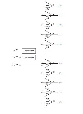
The CDCVF2310PWR is a 2.5V TO 3.3V High-performance clock buffer that operates up to 200 MHz. Two banks of five outputs each provide low-skew copies of CLK.
Parametrics
CDCVF2310PWR absolute maximum ratings: (1)Supply voltage range, VDD: –0.5 V to 4.6 V; (2)Input voltage range, VI: –0.5 V to VDD + 0.5 V; (3)Output voltage range, VO: –0.5 V to VDD + 0.5 V; (4)Input clamp current, IIK (VI < 0 or VI> VDD): ±50 mA; (5)Output clamp current, IOK (VO < 0 or VO > VDD): ±50 mA; (6)Continuous total output current, IO (VO = 0 to VDD): ±50 mA; (7)Package thermal impedance, qJA: PW package 120℃/W; (8)Storage temperature range Tstg: –65℃ to 150℃.
Features
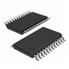
CDCVF2310PWR features: (1)High-Performance 1:10 Clock Driver; (2)Operates up to 200 MHz at VDD 3.3 V; (3)Pin-to-Pin Skew < 100 ps at VDD 3.3 V; (4)VDD Range: 2.3 V to 3.6 V; (5)Operating Temperature Range –40℃ to 85℃; (6)Output Enable Glitch Suppression; (7)Distributes One Clock Input to Two Banks of Five Outputs; (8)25-Ω On-Chip Series Damping Resistors; (9)Packaged in 24-Pin TSSOP.
Diagrams
| Image | Part No | Mfg | Description |  |
Pricing (USD) |
Quantity | ||||||||||||
|---|---|---|---|---|---|---|---|---|---|---|---|---|---|---|---|---|---|---|
 |
 CDCVF2310PWR |
Texas Instruments |
Clock Buffer HP 1:10 Clock Buffer |
Data Sheet |
|
|
||||||||||||
|
CDCVF2310PWRG4 |
Texas Instruments |
Clock Buffer HP 1:10 Clock Buffer |
Data Sheet |
|
|
||||||||||||