(China (Mainland))

Product Summary
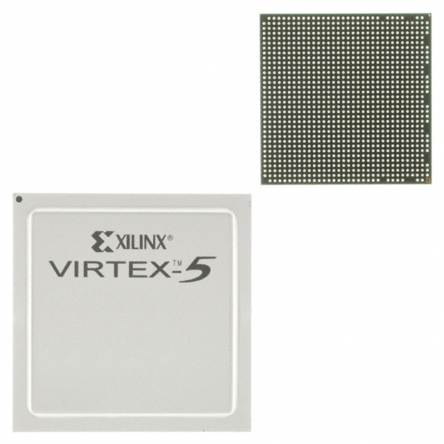
The XC5VLX85-1FFG676C is an FPGA of Virtex-5 family. The XC5VLX85-1FFG676C provides the newest most powerful features in the FPGA market. Using the second generation ASMBL (Advanced Silicon Modular Block) column-based architecture, the XC5VLX85-1FFG676C contains five distinct platforms (sub-families), the most choice offered by any FPGA family. Each platform contains a different ratio of features to address the needs of a wide variety of advanced logic designs. In addition to the most advanced, high-performance logic fabric, the XC5VLX85-1FFG676C contains many hard-IP system level blocks, including powerful 36-Kbit block RAM/FIFOs, second generation 25 x 18 DSP slices, SelectIO technology with built-in digitallycontrolled impedance, ChipSync source-synchronous interface blocks, system monitor functionality, enhanced clock management tiles with integrated DCM (Digital Clock Managers) and phase-locked-loop (PLL) clock generators, and advanced configuration options. Built on a 65-nm state-of-the-art copper process technology, the XC5VLX85-1FFG676C is a programmable alternative to custom ASIC technology.
Parametrics
XC5VLX85-1FFG676C absolute maximum ratings: (1)VCCINT, Internal supply voltage relative to GND: –0.5 to 1.1 V; (2)VCCAUX, Auxiliary supply voltage relative to GND: –0.5 to 3.0 V; (3)VCCO, Output drivers supply voltage relative to GND: –0.5 to 3.75 V; (4)VBATT, Key memory battery backup supply: –0.5 to 4.05 V; (5)VREF, Input reference voltage: –0.5 to 3.75 V; (6)TSTG, Storage temperature (ambient): –65 to 150℃; (7)TSOL, Maximum soldering temperature: +220℃; (8)TJ, Maximum junction temperature: +125℃.
Features
XC5VLX85-1FFG676C absolute maximum ratings: (1)VCCINT, Internal supply voltage relative to GND: –0.5 to 1.1 V; (2)VCCAUX, Auxiliary supply voltage relative to GND: –0.5 to 3.0 V; (3)VCCO, Output drivers supply voltage relative to GND: –0.5 to 3.75 V; (4)VBATT, Key memory battery backup supply: –0.5 to 4.05 V; (5)VREF, Input reference voltage: –0.5 to 3.75 V; (6)TSTG, Storage temperature (ambient): –65 to 150℃; (7)TSOL, Maximum soldering temperature: +220℃; (8)TJ, Maximum junction temperature: +125℃.
Diagrams
| Image | Part No | Mfg | Description |  |
Pricing (USD) |
Quantity | ||||||
|---|---|---|---|---|---|---|---|---|---|---|---|---|
 |
 XC5VLX85-1FFG676C |
|
IC FPGA VIRTEX-5 85K 676FBGA |
Data Sheet |
|
|
||||||
|
XC5VLX85-1FFG676CES |
|
IC FPGA VIRTEX-5 ES 85K 676-FBGA |
Data Sheet |
Negotiable |
|
||||||